34.8 Specialized and research sensors⧉
Everything in this part so far has leaned on a consumer story: the quad-Bayer phone sensor, the dual-pixel autofocus, the time-of-flight module in a tablet. Those are sensors built to a price, to a power budget, and to the constraint that they sit behind a tiny lens in someone's pocket. There is another world of image sensors that faces different versions of those constraints: focal planes built for astronomy, for airborne and space surveillance, for laser radar, for science and defense, where a specialized measurement may justify custom fabrication, cooling, or readout while power, mass, reliability, and cost remain hard constraints. This chapter is a tour of that family of specialized, research, and custom sensors.
A recurring home for this work, in the United States, is MIT Lincoln Laboratory, a federally funded research-and-development center that has designed custom focal-plane arrays (the array of detectors at the image plane, with its readout electronics) since the early days of the charge-coupled device; several exemplars below are Lincoln's. But the family is broader than any one lab; it includes survey-telescope camera builders, aerospace primes, university groups, and the sensor divisions of the big foundries, and the unifying theme is simple: each of these sensors is an ordinary photosite array re-engineered to win along one extreme axis, such as sensitivity, dynamic range, speed, size, curvature, wavelength, or radiation tolerance, at a cost (size, power, price, or cryogenic cooling) that a phone could never pay. Read the chapter as the far end of the spectrum whose near end is the CMOS tricks of Chapter 34.2, Modern sensors (quad Bayer, in-sensor HDR, and beyond): the same design instinct under a different budget.
34.8.1 Geiger-mode avalanche-photodiode arrays: photon-counting laser radar⧉
The first extreme is sensitivity, taken to its physical floor: a sensor that fires on a single photon. The device is the Geiger-mode avalanche photodiode (APD), the same detector class as the single-photon avalanche diode (SPAD) developed in Chapter 34.5, Single-photon sensors (SPAD, avalanche, photon counting). An ordinary photodiode produces a current proportional to the light; an avalanche photodiode runs at a high reverse bias so that one freed photo-electron is accelerated hard enough to knock loose more carriers, multiplying itself into a measurable pulse. Bias it past its breakdown voltage, in Geiger mode, and a single absorbed photon triggers a self-sustaining avalanche: a clean digital click, with a timestamp good to tens or hundreds of picoseconds. Lincoln Laboratory built some of the first large arrays of these detectors, each pixel wired to its own digital timing circuit, in the late 1990s and 2000s Aull et al. 2002.
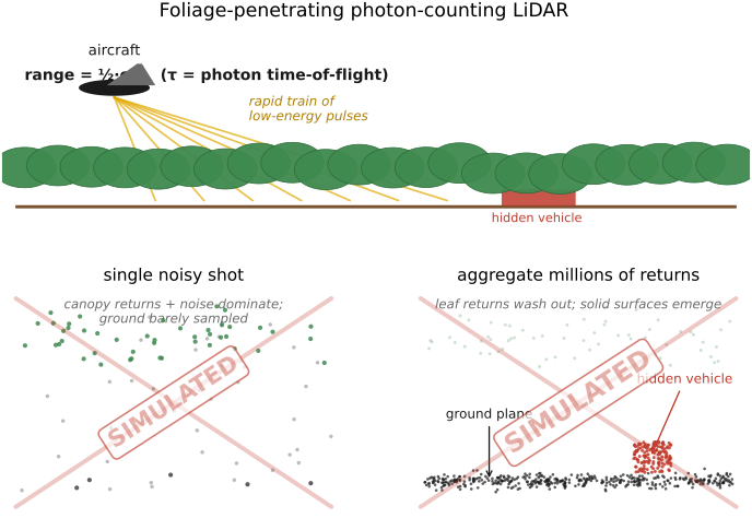
What you do with such an array is direct time-of-flight laser radar, LiDAR, at the photon-counting limit. Fire a short laser pulse, and for each pixel record the arrival time of the first returning photon; the time of flight, multiplied by the speed of light and halved, is the range to whatever that pixel's line of sight hit. Because the detector can register a single photon, sparse returns from repeated shots can be accumulated, which means you can use a low-power laser, scan extremely fast, or reach very long range from an aircraft or satellite.
The application that made this lineage famous is foliage-penetrating 3-D imaging, embodied in Lincoln's airborne "Jigsaw" system Marino & Davis 2005. Fly over a forest firing thousands of laser pulses per second from many slightly different vantage points, and most photons come back off leaves, but a few thread through the gaps in the canopy, reach the ground (or a vehicle hidden under the trees), and return. Any single shot is almost all canopy and noise; but because each return carries a precise 3-D position, you can aggregate millions of sparse single-photon returns into one dense point cloud and then statistically separate the layers. Canopy returns also align in a registered point cloud. The advantage is that range separates canopy and ground layers, while changing viewpoint exposes different gaps. Motion of leaves and weak returns complicate classification rather than automatically canceling the canopy. The result is a 3-D model of the forest floor, and of what is parked on it, reconstructed photon by photon from above an intact canopy. It is the synthetic-aperture see-through idea of Chapter 31.4, Refocusing and synthetic aperture reincarnated in the time domain: instead of shifting and summing rays across a wide aperture to blur away an occluder, you accumulate time-stamped photons across many shots until enough returns through gaps support the hidden surface; the canopy is separated by range and geometry, not made transparent.
34.8.2 Digital-pixel focal-plane arrays⧉
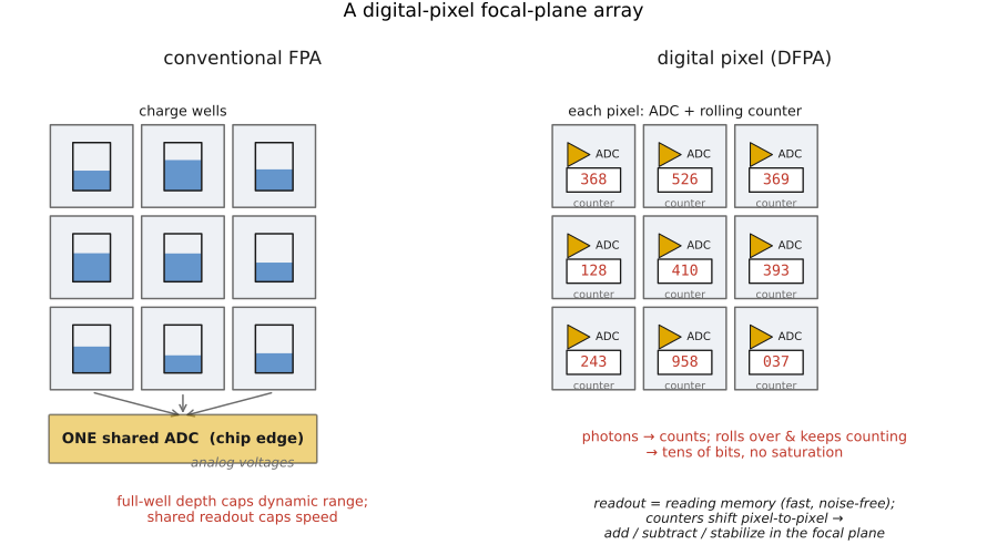
The second extreme is dynamic range, and the trick is to push the analog-to-digital conversion of Chapter 2.7, Sensors: photosites, CCD vs CMOS all the way down into the pixel. A conventional sensor accumulates charge in a well, then reads that charge out as a voltage and digitizes it at the edge of the chip; the well's finite depth (its full-well capacity) caps how much light a pixel can record before it saturates, and the shared readout caps how fast you can get data off. A digital-pixel focal-plane array (DFPA), a Lincoln Laboratory specialty Schultz et al. 2014, puts an analog-to-digital converter and a digital counter inside every pixel. Each pixel converts its own photocurrent to a stream of pulses and counts them in a local register; the counter stores a finite digital total, so the effective full well is no longer the size of a charge bucket but the size of a binary counter, tens of bits and millions of electrons' worth, a large but finite dynamic range. Counter wraparound must be tracked or prevented, and pulse rate and conversion noise impose additional limits. It is the research-grade limit of the counting pixel met among the on-sensor-HDR strategies of Chapter 34.3, On-sensor HDR.
Because each pixel holds its result as a number rather than a fragile analog charge, two more things become possible. First, readout is just reading memory: potentially fast and parallel without adding analog read noise to an already digitized value. Memory bandwidth and the conversion noise already present still limit performance. Second, you can do arithmetic in the focal plane: the on-pixel counters can be made to shift their counts to neighboring pixels in lockstep, which lets the array add, subtract, and even electronically stabilize an image on the sensor, counting up the incoming light while electronically sliding the accumulating image to track a moving scene, so a long exposure of a fast-moving target stays sharp. The pixel has stopped being a passive bucket and become a tiny processor; the boundary between "sensor" and "computer" that we drew back at digitization has dissolved.
34.8.3 Scientific imagers: cryogenic CCDs, sCMOS, and gigapixel mosaics⧉
Astronomy and scientific imaging push sensitivity, noise, and size in their own directions, under demanding power, thermal, and calibration constraints. The classic instrument is the cryogenic scientific CCD: a charge-coupled device cooled to well below freezing (liquid-nitrogen temperatures for the most demanding work) to suppress thermal dark current, read out slowly and quietly so that read noise drops to a handful of electrons, and operated for exposures of minutes to hours to integrate the faint light of distant objects. Their modern complement is the scientific CMOS (sCMOS) sensor, which can combine very low read noise with high frame rates; neither architecture universally has the lower noise floor, the workhorse of live-cell microscopy and fast astronomy. (The same cooling-and-quieting logic, at consumer scale, is why long-exposure and astrophotography cameras actively cool their sensors.)
Wide-area surveillance and survey astronomy then want the largest possible focal plane, tiled from many such CCDs into a single gigapixel mosaic, the kind of array behind survey telescopes, and the optical-instrument cousin of the multiscale gigapixel cameras of the computational-optics part Brady et al. 2012. Lincoln Laboratory's orthogonal-transfer CCD added a twist directly relevant to imaging: it can shift accumulating charge in both directions during the exposure, so that as atmospheric turbulence jitters a star around, the sensor slides the gathering charge to follow it, an on-chip image stabilizer for the night sky, the CCD-era ancestor of the digital-pixel stabilization above Tonry et al. 1997 (the Pan-STARRS gigapixel survey camera is the best-known deployment, and the same wafer-scale ambition runs on into the billion-pixel focal planes of today's survey cameras).
34.8.4 Stacked and processing-in-pixel sensors⧉
A research thread that has now reached consumer silicon is stacking the computer under the sensor. As Chapter 34.2, Modern sensors (quad Bayer, in-sensor HDR, and beyond) describes, a back-side-illuminated (BSI) sensor flips the wafer so light reaches the photodiodes directly, and a stacked sensor bonds that thinned photodiode wafer onto a second wafer of logic beneath it. The specialized/research end of this idea pushes toward processing-in-pixel: dedicating the stacked silicon under (or beside) each pixel to computation as well as readout and ADCs, running a small neural network, event detection, or feature extraction on the focal plane so that only the relevant, already-processed data leaves the chip. This is the architectural limit of the "compute under the pixels" idea, and the meeting point of this chapter's custom focal planes with the on-chip image-signal processing of the mainstream sensor: the difference is one of degree, not kind.
34.8.5 Curved focal planes⧉
A lens naturally focuses a sharp image not onto a flat plane but onto a curved surface (field curvature, an aberration the optics part met); flat sensors fight this with extra lens elements. Bending the silicon itself to match the lens's natural focal surface removes the aberration optically, allowing simpler, faster, wider lenses with near-uniform illumination and sharpness to the corners. Thinning a commercial CMOS die and pneumatically forming it into an accurate spherical surface (without losing function) has been demonstrated in prototype cameras with custom lenses Guenter et al. 2017 (curved image sensor), and several other groups (Lincoln Laboratory among them) have pursued curved focal planes for wide-field imaging. It remains a research and specialty direction rather than a mass-market one, because curving the sensor complicates fabrication and ties each sensor to one lens design.
34.8.6 Beyond the visible, and filter-array sensors⧉
Silicon sees roughly 0.4–1.0 µm. Reaching into the short-, mid-, and long-wave infrared, for night vision, thermal imaging, and spectroscopy, needs different detector materials (indium gallium arsenide, mercury cadmium telluride) hybridized pixel-by-pixel onto a silicon readout chip, with cooling requirements that depend on material and wavelength. Many SWIR arrays operate without cryogenic cooling, and uncooled thermal microbolometers detect heating rather than relying on these photodiodes. Multispectral and hyperspectral focal planes go further, resolving each pixel into many narrow wavelength bands so the sensor measures a spectrum, not a color, the instrument behind remote sensing of crops, minerals, and pollution, and the long-wavelength end of the "color is multiplexing" story from the fundamentals part, taken to dozens or hundreds of bands.
Several of these capabilities are now packaged as filter-array sensors: the idea of Chapter 34.1, Assorted pixels applied to something other than exposure or RGB color. A polarization image sensor tiles a micro-grid of wire-grid polarizers at four orientations over a 2×2 block of pixels, so a single capture yields the local polarization state of the light alongside its intensity Maruyama et al. 2018, useful for cutting glare, separating reflections, and recovering surface orientation (cross-referenced from the polarization-imaging discussion). The same trick puts a multispectral filter mosaic of narrow-band filters directly on the pixel grid, demultiplexed computationally just like a Bayer mosaic. In each case the sensor is ordinary silicon; the cleverness is the patterned filter array and the reconstruction that follows.
34.8.7 Radiation-hardened and defense focal planes⧉
A sensor in orbit or near a reactor is bombarded by particles that flip bits, spike pixels, and slowly degrade silicon. Space and defense focal planes are therefore radiation-hardened, designed and fabricated to reduce single-event failures and tolerate the expected total dose and displacement damage. Radiation hardness is specified for a mission environment; it does not guarantee that every particle hit is harmless or that degradation vanishes. It is a robustness axis with essentially no consumer analog, and one where the custom-focal-plane labs (Lincoln Laboratory and the aerospace primes among them) do much of the work.
34.8.8 The chapter's point⧉
The thread through all of these: a focal plane is not a fixed thing. Choose an axis such as single-photon sensitivity, counts-per-pixel dynamic range, frame rate, format, curvature, wavelength, polarization, radiation tolerance, or on-chip computation, and there is a sensor engineered to win it, usually at a size, power, and cost that only a telescope, an aircraft, a satellite, or a lab can carry. The consumer CMOS sensor and these specialized focal planes are the same idea at opposite ends of the budget: measure light better than the default by building a smarter pixel.