34.2 Modern sensors (quad Bayer, in-sensor HDR, and beyond)⧉
A phone's main camera advertises a startling pixel count, 48, 50, 108, even 200 megapixels, on a sensor a fingernail wide. Those counts describe photosites, not independent resolved color samples. Small pixels can supply useful detail in good light, but their per-pixel signal-to-noise ratio and the lens response constrain the result. The numbers make sense only once you understand that the pixels are raw material, not the final image. A modern sensor's photosites are deliberately small and numerous so that the camera can choose acquisition and readout modes to spend them: combine them for a clean low-light frame, read them at staggered exposures for dynamic range, split them for autofocus, or, in bright light, read them all out for genuine high resolution. The mosaic and the pixel have become programmable. This chapter is about the handful of architectural moves that make that possible.
34.2.1 Quad Bayer, Tetracell, and nona-binning⧉
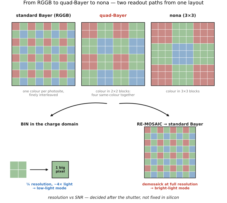
The foundational move is to abandon the strict one-color-per-pixel Bayer tile and instead group same-color pixels together. In a quad-Bayer mosaic (Samsung markets it as Tetracell, Sony as Quad Bayer), the color filters are laid down not one pixel at a time but in 2×2 blocks: a 2×2 patch of red, beside a 2×2 of green, and so on, so each color filter covers four photosites instead of one (Figure 34.2.1). A nona (3×3, "Nonacell") or even tetra²/16-cell (4×4) variant groups nine or sixteen. The point of clustering same-color pixels is that the camera can now treat each cluster two completely different ways depending on the light:
- Bin, in low light. Combine the four same-color photosites into one large effective pixel. The result is a quarter-resolution image (a 48 MP sensor reports 12 MP) with roughly four times the photoelectrons per output pixel and twice the shot-noise-limited SNR of one small pixel, the clean low-light mode.
- Re-mosaic, in good light. Read all four sub-pixels separately and computationally rearrange the quad layout into a standard Bayer pattern, producing a full-size mosaic estimate to feed an ordinary demosaicker.
This is the resolution-versus-SNR decision of Chapter 2.8, Noise, signal-to-noise ratio and dynamic range (an instance of the full-well/noise-floor trade) made programmatically, frame by frame, instead of being frozen into the sensor. Bright scene: take the megapixels. Dim scene: take the SNR.
Where the binning gain comes from, and where it leaks. As the noise chapter establishes, summing four same-color pixels recovers the same shot noise as one big pixel that caught the same photons, regardless of how you combine them, but the read noise is paid once per read-out. Pooling charge before a single read can avoid accumulating several read-noise contributions. With four independent reads of equal variance, the summed read-noise variance is four times that of one read, so its standard deviation is twice as large. Digital binning still improves SNR over a single small pixel. Actual gains depend on conversion gain, capacitance, correlated noise, and the sensor's charge-, voltage-, or digital-domain implementation.
The re-mosaic problem and its artifacts. Re-mosaicking is not free. The quad layout samples each color in clumps of four, so converting it to the finely-interleaved standard Bayer field is an interpolation/super-resolution problem, and it struggles in the same places as Bayer demosaicking, especially on fine, high-frequency texture and sharp edges, where the clumped sampling can produce false color and zipper/maze artifacts or a slightly soft result. It also adds a front-end stage to the pipeline: the raw quad data must be re-mosaicked before the conventional step of Part 15, Demosaicking and joint methods can run.
34.2.2 In-sensor HDR: capturing range before the merge⧉
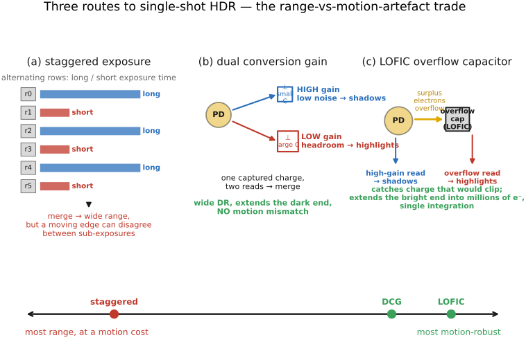
The same clustered, programmable pixels open a second door: instead of (or as well as) trading resolution for light, trade it for dynamic range, capturing a high-range scene in essentially one shot and sidestepping the inter-frame ghosting of multi-exposure HDR merging. There are four routes, sitting at different points on the dynamic-range-versus-motion-artifact trade (Figure 34.2.2).
1. Staggered exposure (DOL-HDR). Acquire long and short sub-exposures with closely scheduled rolling readouts, then merge them in the downstream processor or, where supported, on the sensor. DOL output can interleave lines belonging to distinct full-resolution exposures; this is not the same as assigning alternate scene rows permanently to different exposure times. Bandwidth and motion mismatch are the principal costs. Spatially varying exposure is a separate option, described in Chapter 34.1, Assorted pixels, and does trade spatial samples for exposure levels.
2. Dual conversion gain (DCG). Give each pixel two read paths: a high-conversion-gain path (small floating-diffusion capacitance → large voltage per electron → low read noise, for the shadows) and a low-conversion-gain path (large capacitance → more highlight headroom before saturation). Reading the same captured charge through both and combining them widens dynamic range at the dark end without a second exposure, so there is no motion mismatch at all, since it is one integration read two ways. A camera may instead select one conversion-gain mode per exposure; that switching capability alone does not imply simultaneous HDR from both reads. (This is the same DCG met in Chapter 2.8, Noise, signal-to-noise ratio and dynamic range.)
3. Lateral overflow integration capacitor (LOFIC). Widen the range at the bright end by refusing to discard the bright charge. Each pixel gets a second reservoir beside the photodiode; as the photodiode nears saturation, surplus electrons overflow into the capacitor instead of clipping, and at read-out the pixel is sampled both ways: a quiet high-gain read for the shadows and the overflow capacitor for the highlights, and merged into one value Akahane et al. 2006. Large-capacity implementations can reach millions of electrons and dynamic ranges above 100 dB (about 16.6 stops), although neither figure applies to every LOFIC pixel with no bracketing and no motion ghosts. LOFIC took hold first in automotive sensors (where flickering LED signage and fast motion make multi-shot HDR untenable) and, by the mid-2020s, in flagship phone sensors. The newest designs stack LOFIC with DCG, reading three signals from one pixel to cover shadows, midtones, and highlights at once.
4. Quad-exposure. Use the quad-Bayer 2×2 cell directly: expose its four same-color sub-pixels for different durations and merge. This folds HDR and the binning machinery into one structure: the cell that bins for low light can instead bracket for dynamic range.
The unifying picture: each method shortcuts the multi-frame HDR merge by capturing the range on the sensor, and they line up on a spectrum from most motion-robust (DCG and LOFIC, which use one integration with no temporal mismatch) to most range-at-a-cost (staggered and quad-exposure, which use separate sub-exposures, so a moving edge can disagree between them). We meet the multi-shot HDR these methods short-circuit in HDR merging and Chapter 17.6, HDR+ and burst imaging on phones.
34.2.3 Dual-pixel autofocus, on the same sensor⧉
The clustered modern pixel also carries the dual-pixel structure of the previous chapter: split each photosite under its shared microlens so the two halves sample opposite halves of the lens aperture, yielding phase-detection autofocus at thousands of points and a faint two-view depth cue, with the halves summed for a full-brightness image and no light lost (Chapter 34.1, Assorted pixels; Chapter 22.9, Autofocus). What is new in the modern sensor is that this lives alongside binning and HDR on one chip, and that fast read-out is what makes continuous, frame-rate PDAF practical. That brings us to the architecture underneath these tricks.
34.2.4 BSI and stacked sensors: compute under the pixels⧉
Fast readout makes these modes practical. Back-side illumination primarily improves optical access to the photodiode; wafer stacking provides room for readout and processing circuitry. A front-illuminated pixel forces light past the metal wiring before it reaches the photodiode, wasting fill factor; a back-side-illuminated (BSI) sensor flips the wafer so light hits the photodiodes directly, with the wiring behind, which is essential once pixels shrink below a micron, and the reason sub-micron quad-Bayer pixels work at all.
Stacking goes further: bond the thinned photodiode wafer on top of a second wafer of logic beneath it, connected by dense through-silicon or hybrid bonds. Now the silicon real estate under the pixels is no longer wasted on wiring; it holds column-parallel ADCs, selected processing logic and, in some designs, a separate DRAM layer. A complete image-signal processor need not be on the sensor. This is the literal meaning of computational sensor: compute under the pixels. That enables the capabilities this chapter has been describing:
- High frame rate and fast read-out, because thousands of ADCs digitize in parallel right beneath the array, enabling the staggered-exposure HDR and the frame-rate PDAF above.
- A layer of stacked DRAM that can dump an entire frame off the pixel array almost instantly and read it out from memory at leisure, giving near-global-shutter read-out that tames rolling-shutter skew, and blackout-free electronic viewfinders.
- On-chip processing: binning, re-mosaic, and HDR merge done on the sensor before the data ever leaves it.
34.2.5 The global-versus-rolling shutter trade⧉
That last point lands on the one trade the modern sensor still cannot fully escape. As Chapter 2.7, Sensors — photosites, CCD vs CMOS details, many CMOS sensors use rolling exposure timing, so each row's exposure window is shifted slightly later than the one above, the rolling shutter, which skews fast motion, wobbles handheld video, and bands under flashes and flickering LEDs. A true global shutter integrates every row over the same time interval, eliminating exposure skew. It does not eliminate motion blur or all flicker effects, but it demands extra in-pixel storage (a shielded memory node per pixel to hold the charge while the array is read), which costs transistor area, fill factor, and often dynamic range. The middle path that stacking enables is the fast/near-global read-out above: dump the whole frame into stacked DRAM so quickly that the row-to-row time skew shrinks to near-imperceptibility, giving most of the benefit of a global shutter without paying its full per-pixel price. As of the mid-2020s, true global-shutter full-frame sensors exist but remain specialized; many cameras instead use faster rolling readout. Whether artifacts are acceptable depends on readout time, subject motion, and illumination flicker.
34.2.6 Beyond: nano-prism, organic, and event pixels⧉
The architectural frontier keeps moving. A nano-prism (color router / split-pixel) replaces the absorptive color filter with an inverse-designed nanostructure that redirects each wavelength to a neighboring photodiode instead of absorbing it, aiming to recover light that absorptive filters reject. Efficiency depends on wavelength, incidence angle, crosstalk, and the chosen definition of useful routed light [@nishiwaki-etal-2013; @zou-etal-2022]. Organic photoconductive films separate light conversion from silicon readout and can offer high charge capacity. An organic conversion layer alone does not eliminate the need for color separation; mosaic-free color needs additional spectral selectivity or layers. And the event (dynamic-vision) pixel abandons the frame entirely, each pixel emitting asynchronous, microsecond-timestamped change events (detailed in Chapter 34.7, Event sensors). The headline megapixel number hides the main point of this chapter: the modern sensor's gains come less from quieter pixels than from making the pixel programmable and getting its data off the chip fast enough for computation to finish the job.