2.5 Sensors: photosites, CCD vs CMOS⧉
We have been treating the pixel as an abstraction: a number that integrates incoming light over a little patch of the image. It is time to look at the thing that actually produces that number — the image sensor — because how it is built, and above all how it is read, quietly decides a great deal of what a camera can and cannot do. The previous chapter owned three axes of the pixel integral (the aperture, the pixel's area, and wavelength); this chapter owns the fourth, time, and the mechanism that opens and closes it: the shutter.
2.5.1 Photon to number: the photosite⧉
A digital sensor is a two-dimensional array of photosites, one per pixel. Each photosite is essentially a tiny bucket — a potential well — that counts photons: arriving light frees electrons, the well accumulates that charge, and at the end of the exposure the charge is converted to a voltage and then, by an analog-to-digital converter (ADC), to a number. Because the well literally counts arrivals, the number it reports is, to good approximation, linear in the amount of light that fell on it. That linearity is not a minor technical detail: it is what lets us treat a raw image as a calibrated radiometric measurement, and it is the foundation that makes HDR merging, deblurring, and depth estimation meaningful later in the book.
It is worth separating two revolutions that are often conflated. The first was electronic imaging: turning light into an analog electrical signal (the era of the CCD and analog video). The second, the one computational photography lives on, was digital: putting an ADC in the path so the signal becomes numbers we can compute on. A sensor that captures light electronically but never digitizes it is a television camera, not a computer's eye.
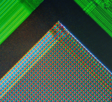
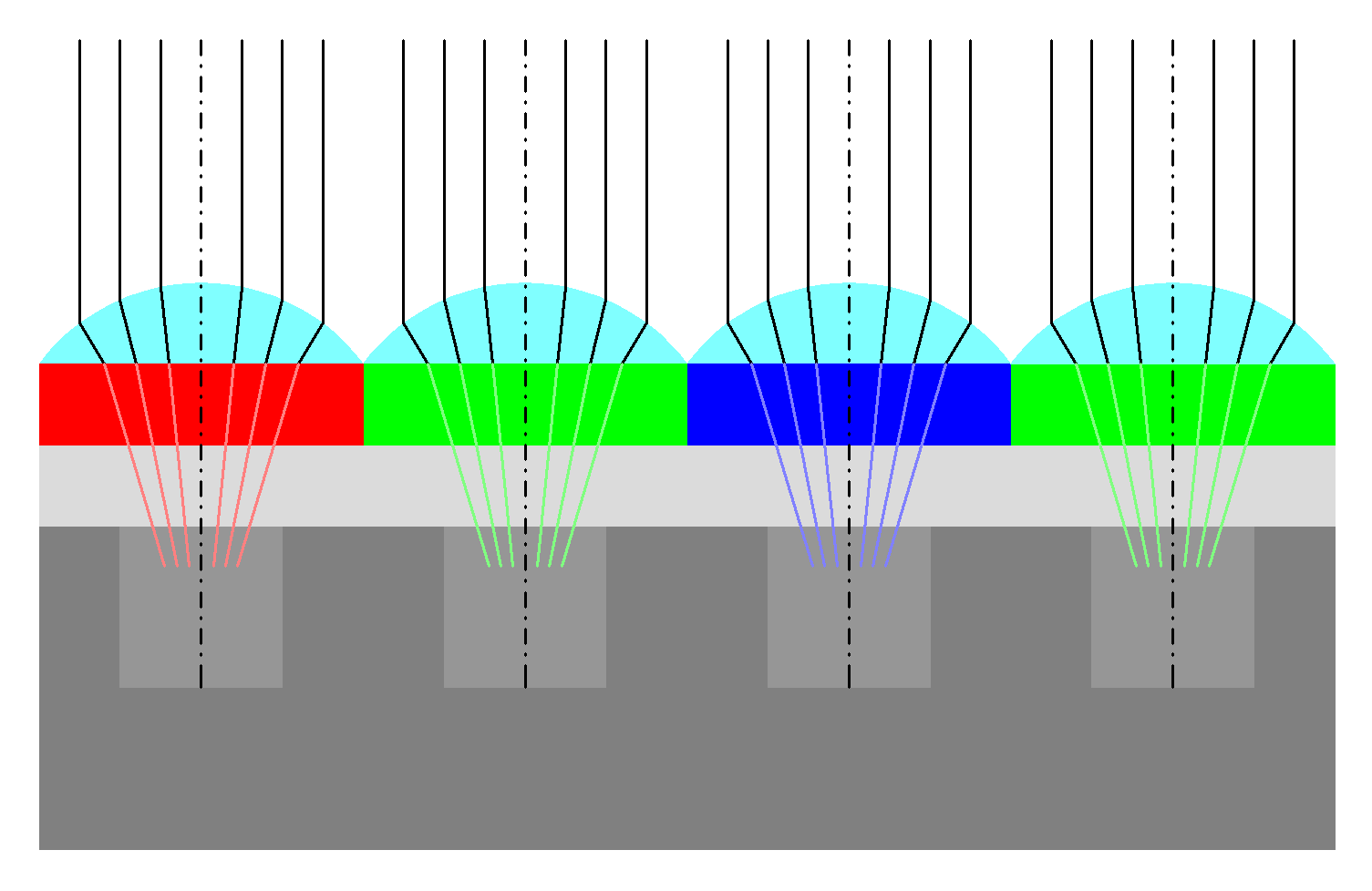
Above each photosite sits a microlens that funnels light onto the light-sensitive area — necessary because wiring occupies part of each pixel, so the fill factor is less than 100%. Under the microlens sits a colour filter, and the mosaic of red, green, and blue filters (the Bayer pattern) is why colour must be reconstructed by demosaicking (a later chapter). Finally, the map from scene radiance to the rendered pixel value is the camera response curve: raw is roughly linear, while a JPEG has a non-linear curve (gamma plus a tone curve) baked in — recovering that curve is exactly the problem HDR has to solve.

2.5.2 CCD versus CMOS⧉
For decades the dominant sensor was the CCD (charge-coupled device). A CCD has no per-pixel electronics; instead it shuttles the accumulated charge across the chip in a "bucket brigade" to a single amplifier at the edge, where it is measured. This makes CCD output clean and uniform, and because the whole frame is transferred together it is naturally a global capture — but it is slow, power-hungry, and cannot put much intelligence on the chip.
The CMOS sensor, now utterly dominant, puts an amplifier — and increasingly the ADC and digital logic — at every pixel, and reads the array out row by row like memory. This is cheap, fast, and low-power, and it is what makes modern computational sensors possible: on-chip ADCs, high-frame-rate and region-of-interest readout, on-sensor HDR, phase-detect autofocus, and pixel binning. The price of reading row by row is that different rows are captured at slightly different times — the rolling shutter, which we return to below.
2.5.3 Time integration: the exposure⧉
Over the exposure time $\Delta t$, the well accumulates photons, so the pixel value is the time integral of the irradiance it receives: $\text{value} \propto \int_0^{\Delta t} E\,dt$. This is the fourth axis of the pixel integral, and it is governed by two controls — the aperture (how much light per unit time) and the exposure time — with ISO applying gain after capture. The familiar trade, exposure = irradiance × time, means halving the light and doubling the time gives the same exposure (reciprocity); digital sensors obey this far more faithfully than film, whose reciprocity failure at long exposures was a perennial nuisance.
The time integral is motion blur: anything that moves during $\Delta t$ is averaged along its path. A long exposure smears motion into light trails and silky water; a short one freezes a hummingbird's wings. Choosing, exploiting, and later undoing this integral is the subject of the motion and deblurring chapters. What ends the integral — cleanly or not — is the shutter.
2.5.4 Mechanical versus electronic shutter⧉
A mechanical shutter is a physical barrier that times the exposure. A leaf shutter, built into the lens, opens from the centre outward and exposes the whole frame at once, so it behaves globally and can synchronize a flash at any speed. A focal-plane shutter, just in front of the sensor, uses two curtains: at short exposures the second curtain begins to close before the first has fully opened, so only a moving slit ever crosses the frame — already a kind of rolling exposure realized in hardware, and the origin of a camera's flash sync speed.
An electronic shutter has no moving parts: the sensor electronically resets each photosite to begin its integration and reads it out to end it. It is silent, free of vibration, and can reach very short exposures and high frame rates. Its drawback on CMOS is that the reset-and-read happens row by row, making it a rolling shutter. Many cameras therefore use an electronic first curtain — an electronic start with a mechanical finish — to avoid shutter-shock blur while keeping a clean ending.
2.5.5 Global, rolling, and readout shutter⧉
The crucial distinction is when each row is exposed.
A global shutter exposes every row over the same time window — all rows start and stop together — and only then reads the frame out. A moving object is captured at a single instant, undistorted. CCDs are global by nature, and special global-shutter CMOS sensors exist, at the cost of extra transistors and area per pixel.
A rolling shutter exposes and reads rows one after another, so each row's time window is shifted slightly later than the row above it. This is cheap and standard on CMOS, but it means the bottom of the frame is seen later than the top. The consequences are a family of artifacts, all from the same cause — different rows, different times: a fast pan or a passing car leans over (skew); handheld video wobbles ("jello"); a spinning propeller or a plucked guitar string takes on surreal, impossible shapes; and a brief flash lights only the rows that happen to be open at that instant, leaving a bright band across the frame (which is precisely why flash sync speed exists).

Artificial light adds its own version. Mains-powered lamps and many LED/PWM sources flicker at 100–120 Hz (or faster, when dimmed by pulse-width modulation). Under a rolling shutter, rows captured at different phases of that flicker receive different amounts of light, producing horizontal brightness banding (and colour banding if the source's phosphors lag). Cameras fight it with anti-flicker modes that time the readout to the flicker period, by matching the exposure to a multiple of that period, or by using a global shutter outright. And when the artifact cannot be prevented, it can be corrected computationally — by estimating each row's time offset together with the camera and scene motion and warping every row back to a common instant, the subject of the video-stabilization chapter.
2.5.6 A taste of modern sensor tricks⧉
CMOS's per-pixel intelligence enables a small zoo of tricks that recur later.
Dual conversion gain and dual native ISO. A CMOS pixel has a degree of freedom that is invisible in a raw file but shapes its noise: the conversion gain, the voltage swing per collected electron at the readout node, set by the node's capacitance. A smaller capacitance gives a larger voltage per electron — high-conversion-gain (HCG) mode — making the amplifier's noise floor small relative to signal: low read noise, ideal for dark scenes and high ISO. A larger capacitance keeps the well deeper before saturation — low-conversion-gain (LCG) mode — at the cost of higher read noise but with much more highlight headroom. A camera that can switch between the two effectively has two native ISOs (e.g. ISO 800 and ISO 12800), and reading or combining both at once extends the dynamic range of a single exposure (→ Noise, signal-to-noise ratio and dynamic range). This is dual conversion gain (DCG).
Quad-Bayer and high-megapixel phone sensors. Many high-megapixel phone sensors — 48, 50, or 108 MP — use a quad-Bayer mosaic (also marketed as Tetracell or quad CFA) that groups 2×2 same-colour photosites under a single colour filter. In good light the four sub-pixels are read separately and remosaiced into a standard Bayer pattern, recovering full resolution; in low light they are binned into one larger effective pixel, trading resolution for ~4× better light collection and a lower noise floor (so a 48 MP sensor delivers clean 12 MP low-light output). The 2×2 group can also be exposed at two different times for in-pixel staggered HDR; a 3×3 variant, the Nonacell, bins nine cells. These sensors need an extra front-end remosaic step that converts the 2×2 (or 3×3) groups into a conventional Bayer mosaic before demosaicking (→ Demosaicking).
Dual-pixel and quad-pixel autofocus. The microlens over a photosite can be shared across two (dual-pixel) or four (quad-pixel, 2×2 on-chip lens) sub-photodiodes, each seeing a different half or quadrant of the lens's exit pupil. Because the two pupil halves form slightly shifted images — exactly a stereo pair — the difference between the sub-diode signals carries a phase proportional to defocus: phase-detection autofocus (PDAF) at every pixel, with no dedicated AF sensor. For the final image the sub-diodes are simply summed, so no light is lost; a quad-pixel (2×2 OCL) arrangement adds sensitivity to both horizontal and vertical phase. The optics and focusing algorithm are in Focus, autofocus.
The deeper menagerie — stacked sensors, event cameras, single-photon avalanche diodes — waits in the Advanced part. (The off-axis cos⁴ natural vignetting met in the previous chapter is a related geometry effect, not a sensor trick.)